Digital bus and interface standards

Efficient eye diagram testing in DDR3/DDR4 system designs

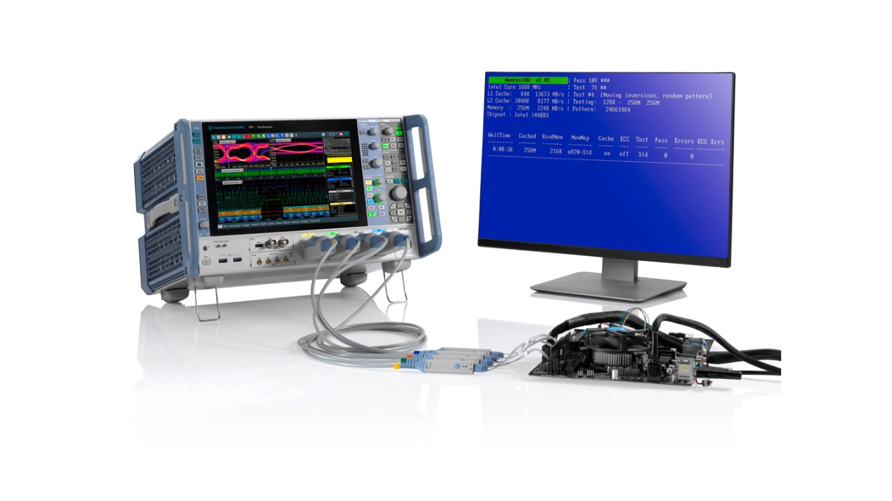
Compliance testing is essential to ensuring that dynamic random access memory (DRAM) signals meet the JEDEC specifications for parameters such as timing, slew rates and voltage levels. For system verification and debugging, eye diagram measurements are the most important tools for efficiently analyzing the signal integrity in any digital design. The specific nature of DDR requires a dedicated solution with a powerful read/write separation to get meaningful eye diagrams on the DDR data bus.

DDR4 system test: read/write separation and DQ data eye
Open Lightbox

Your task

When testing the signal quality on a DDR interface, eye diagram measurements on the data, command/address and control signals help to reveal and troubleshoot potential signal integrity issues in the system. Therefore, the eye diagram function is very popular among many SI engineers because it enables them to quickly determine the DDR interface performance. While compliance tests verify the signal characteristics of the DDR signal groups in accordance with the JEDEC specifications, they lack the flexibility to efficiently analyze and debug signal integrity issues. Here, the eye diagram measurement is the tool of choice. For the unidirectional command/address and control signal groups, no read/write separation is required.

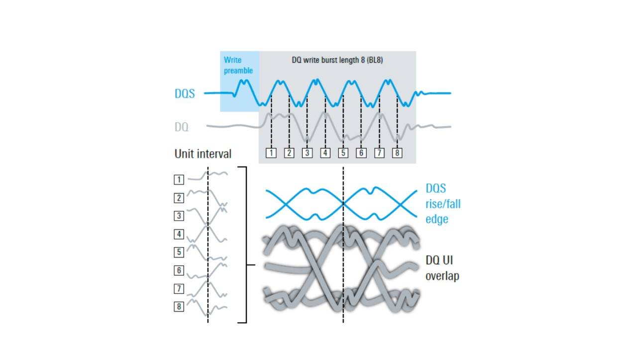
However, since the data bus facilitates a bidirectional data transfer between memory controller and memory device, building the data eye requires a powerful read/write separation along with the overlapping of consecutive bits within the data bursts.

DQ eye diagram overlaps UIs within a burst length
Open Lightbox

Rohde & Schwarz solution

The R&S®RTx-K91 (DDR3, DDR3L, LPDDR3) and R&S®RTx-K93 (DDR4, LPDDR4) signal integrity and compliance test software options feature comprehensive, automated DDR and LPDDR compliance tests, including an additional function to efficiently separate read/write bursts and measure the DDR data eye.

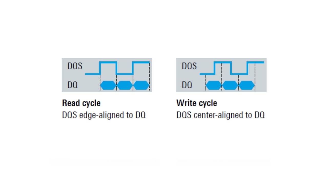
Phase alignment of DQS and DQ signals
Open Lightbox

DDR data eye: separating read/write bursts

The R&S®RTx-K91 and R&S®RTx-K93 options come with a decoding function that helps to distinguish all read/write cycles in the acquired waveforms.

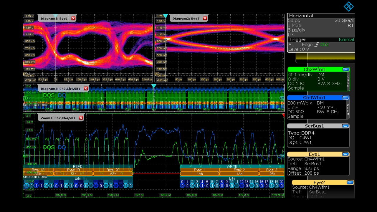
This decoding function identifies and separates read and write data bursts, analyzing phase alignment and signal level of the DQ and DQS signals on the measured data bus. It synchronizes the DQ data eye to the DQS strobe signal. DDR3 and DDR4 read/write data bursts also include a preamble that needs to be excluded from the eye diagram. The R&S®RTx-K91 and R&S®RTx-K93 options intelligently detect and omit the preamble prior to the data burst to form a proper eye diagram suitable for testing.

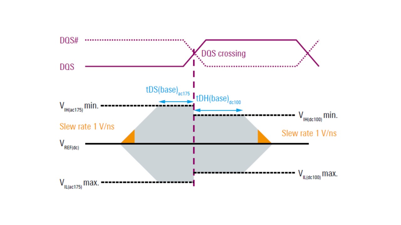
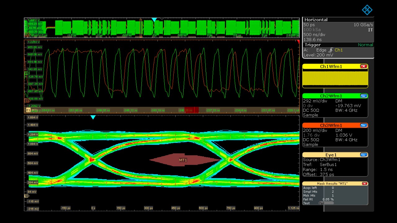
Example of defining an eye mask for DDR3
Open Lightbox

The separation and decoding of read/write bursts is solely based on DQ and DQS phase relationship and threshold hysteresis without the need to probe additional control signals. Users can capture a longer duration of DQ bursts to create a write- and/or read-only eye diagram for testing. Once an eye diagram is established, analysis tools such as mask test, histogram and automated eye measurements can be applied.

R&S®RTP-K93: separation and decoding of read and write data bursts
Open Lightbox

Eye masks in DDR3 and DDR4

Even though not included in all DDR specifications, eye diagrams are the tools of choice for interface verification and debugging in DDR3 and DDR4 system designs. Whereas DDR4 defines the corresponding eye mask parameters for the DQ data signal, DDR3 does not specify a mask for the DQ data eye. However, a DDR3 eye mask can be derived from the JEDEC specification using the data setup (tDS) and hold time (tDH) to define the width of the eye; slew rate and voltage levels (VIH and VIL) define the vertical eye opening. This methodology to construct the mask can be efficiently used for testing the signal integrity on the data bus, even for DDR3 system designs. Note that in the DDR3 specification, the signal timing and level requirements depend on the actual signal slew rates as well as the selected reference level and data rates. Therefore, the user will need to configure the data mask according to the device characteristics.

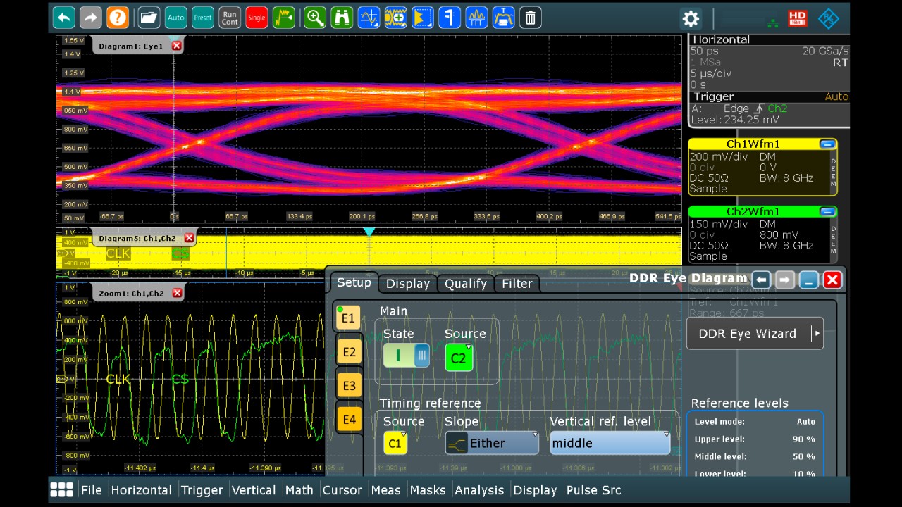
R&S®RTP-K93: DDR4 eye diagram of chip select signal (CS)
Open Lightbox

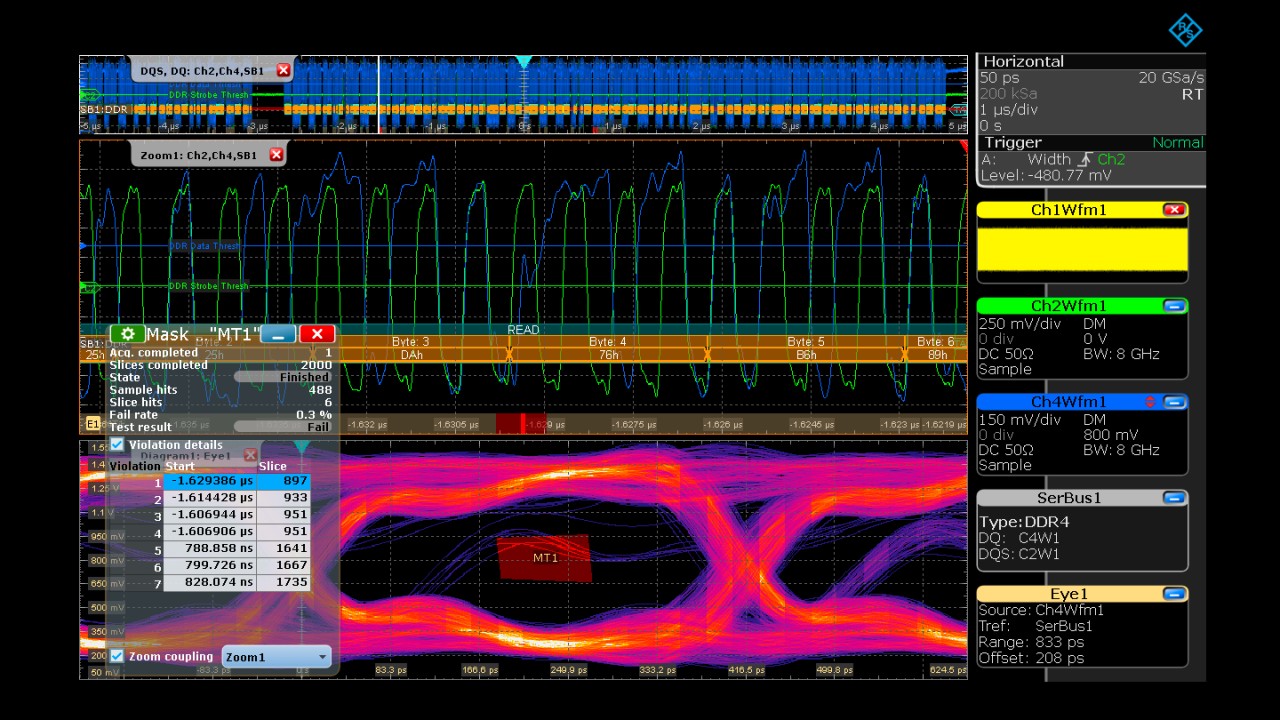
The R&S®RTP and R&S®RTO oscilloscope standard mask test function works together with the R&S®RTx-K91 and R&S®RTx-K93 DDR data eye diagram tool. Users can define required mask profiles and save them for later testing. Violations of the mask are indicated on the waveform (eye stripe function) and can be tabulated based on UI sequences. Users can zoom into individual mask violations to further analyze and debug signal integrity issues.

R&S®RTP-K93: DDR4 DQ data eye and mask test with indication of violation area (example of read cycle)
Open Lightbox

Further eye diagrams in DDR

In contrast to the bidirectional data bus, the command/address and control signals are unidirectional and do not require read/write separation. These signals are synchronized to the clock signal CK. Eye masks and mask tests can be configured in the same way as for the data bus.

R&S®RTP-K91: DDR3 DQ data eye and mask test with indication of violation area (example of write cycle)
Open Lightbox

Summary

In DDR3 and DDR4 memory interface testing, compliance tests help to benchmark the interoperability against the JEDEC standard. When debugging SI issues, features and tools such as read/write detection, eye diagrams and mask tests are needed to facilitate the analysis effort. The R&S®RTx-K91 and R&S®RTx-K93 options offer a powerful toolbox for compliance testing as well as verification and debugging of DDR3 and DDR4 system designs.

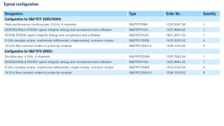
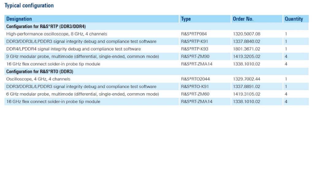
Typical configuration
Related solutions