Ground or no ground, that is the question – how to connect your probe

High-speed serial interfaces often transmit data with differential signaling and differential probes that can be used to access signal traces. In addition to differential inputs, these probes have a ground connection.

One important question when connecting R&S®RT‑ZMxx modular multimode probes is whether or not to connect the probe ground (GND) to the device under test (DUT).

Rohde & Schwarz solution

The R&S®RTP high-performance oscilloscope is an ideal, one-box solution for high-speed digital interface testing. R&S®RT-ZMxx modular probes together with a wide range of probe tips (R&S®RT-ZMAxx) and accessories can help you easily access data signals and master mechanical and electrical connection challenges for increased measurement confidence.

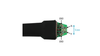
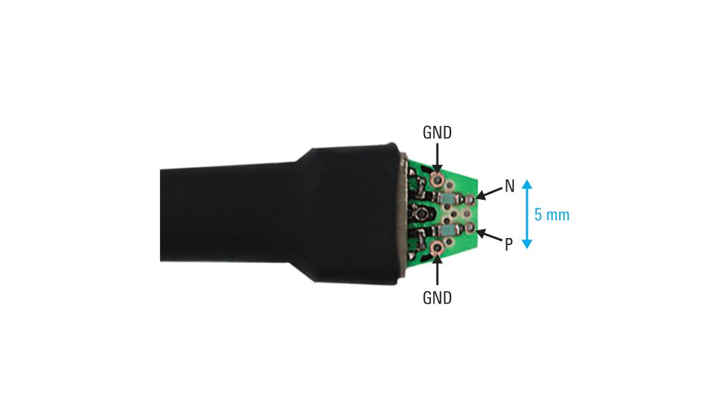
Figure 1: R&S®RT-ZMA10 solder-in probe tip
Open Lightbox

Application

When testing high-speed digital interfaces, the circuit connection is crucial to measurements. First you need to decide whether to analyze a host-to-device (or vice versa) data signal or to test for compliance. When analyzing a host-to-device data signal, a R&S®RT-ZM160 probe can be used to tap the live signal. Compliance testing requires a standard-complaint test fixture that can access the signal using standard 50 Ω equipment (cable, connector, balun, …).

This application card looks at data signal analysis for a conventional USB 3.2 generation 1 memory flash drive. After checking all the parameters, such as bandwidth, operating voltage window and loading, take the R&S®RT-ZM160 and a R& S®RT-ZMA10 probe tip and solder the probe tip (see Figure 1) with P, N, GND to the USB interface on the memory flash drive (TX port) and connect the flash drive to a desktop computer.

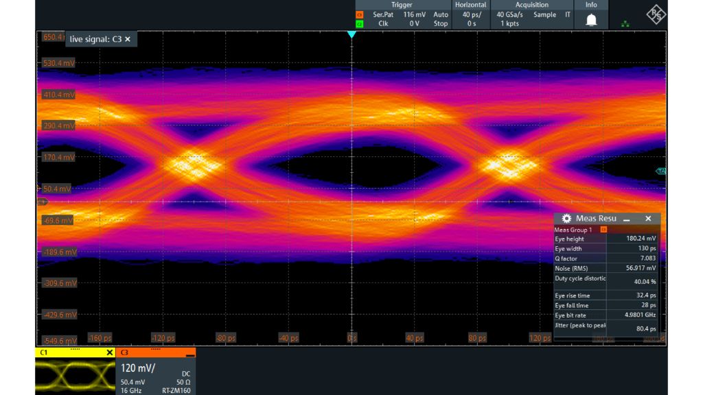
Figure 2: Eye pattern of the differential signal after connecting P, N, GND
Open Lightbox

First check the integrity of the differential signal (DM mode) with an eye pattern test (see Figure 2). The eye pattern here reveals a few flaws. The eye has high jitter even though the device is connected right at the transmitter, the Q factor is low, while the differential signal has an offset and is not symmetrical around 0 V.

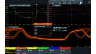
Start by investigating the DC issue and find out why bias appears on the differential signal. Set a width trigger (1 ns) to capture five bits of the same polarity for the frequently occurring SKP (K28.1) character. Now the traces for the differential, common-mode, p and n will be acquired (see Figure 3). The probe meter and a mean measurement for the common-mode signal were enabled to test DC parameters.

Figure 3: Separating the signal into differential (R1), common-mode (R2), P (R3), and N (R4) parts(
Open Lightbox

You may notice that the p and n traces are roughly symmetrical to the common mode-trace. This raises two questions. First, if p and n are symmetrical around a DC value (CM signal in green), the differential trace should be symmetrical around 0 V, since the DC value is canceled out. Second, the common-mode value (6 mV) of the probe meter and the value (137 mV) of the mean measurement for the common-mode signal do not match. With this in mind, review the entire circuit beyond the usual high-speed traces. Including the power supply connections (see Figure 4) can be helpful along with using a digital multimeter to check resistance between the easily accessible USB shield and the oscilloscope ground of less than 10 mΩ with a disconnected Probe.

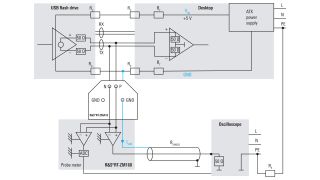
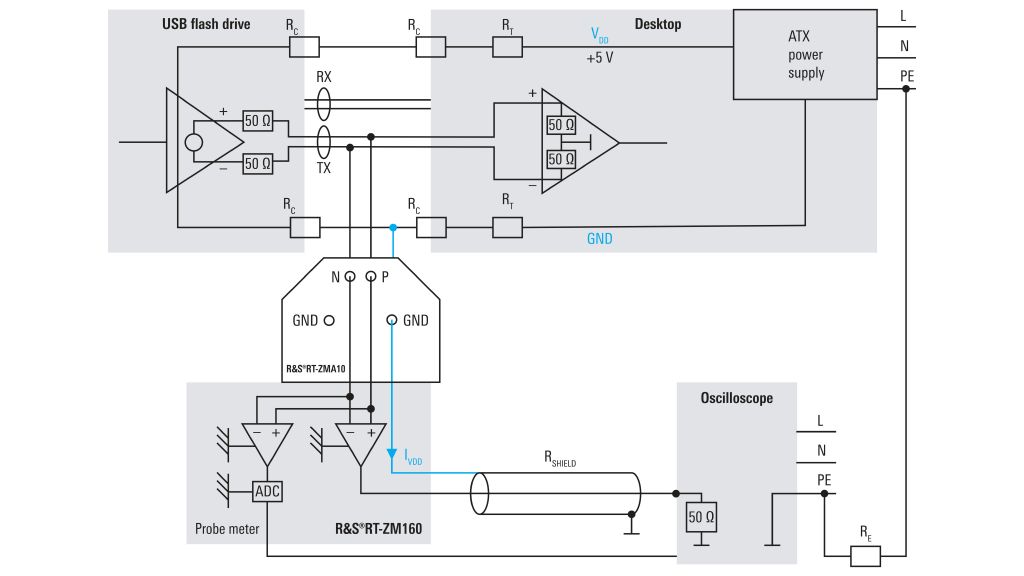
The desktop, the USB flash drive and the oscilloscope with the R&S®RT-ZM probe are illustrated on the equivalent circuit diagram (see Figure 4). The relevant supply voltage, i.e. the USB bus voltage (VDD 5 V), is shown along with the USB high-speed RX and TX connections. The supply trace resistance values are introduced (RE, Rshield, RT, RC) together with the supply voltages.

Figure 4: Equivalent circuit
Open Lightbox

RE stands for the resistive load of the protective earth (< 10 mΩ). Rshield is the shield resistance of the probe cable (about 30 mΩ). RT is the host trace resistance (max. 167 mΩ) and RC is the mated connector resistance (max. 30 mΩ). Both RT and RC are stipulated in the USB 3.2 specification chapter 11.4.2 (see table below). RT, RC together with RE and Rshield form a current divider for the ground current in the USB flash drive when the blue-marked ground connection in the probe tip is connected. In the following, the influence of the network is estimated and implementation is assumed to have a third of the maximum value for the RT and RC specs. This means the values are roughly those of RE or Rshield resistors.

Significant DC current is marked as IVDD and flows over the probe coaxial shield. Assuming 500 mA supply current is extracted from the USB driver data, the current through the probe and oscilloscope is estimated at 300 mA, resulting in an IR drop of 9 mV along the probe cable shield.

Since the amplifier in the probe tip is referenced to the local ground and the oscilloscope input to the common ground, the difference in potential between the tip and chassis is 9 mV. This may seem slight, but the probe attenuates at 10:1 or 2:1 depending on the vertical scale. Here, the software multiplies all voltages from the input ports with a connected probe using the reciprocal attenuation and the 9 mV difference becomes 90 mV with 10:1 attenuation.

This effect is apparent in the differential signal, since the signal is converted from a differential to single ended signal in the probe tip amplifier, with the local, probe ground reference and the 9 mV potential shift added later.

Another side effect comes from the analog-digital converter (ADC) in the oscilloscope signal path being referenced to the common ground, whereas the ADC in the probe meter is referenced to the local DUT ground, creating the observed difference in common mode voltage (6 mV versus 137 mV).

USB maximum supply resistance
Host trace resistance RT 167 mΩ
Mated connector resistance RC 30 mΩ
Cable resistance RW 190 mΩ
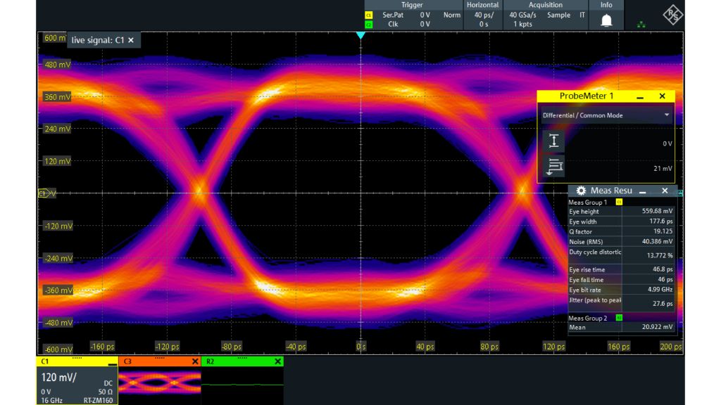
Figure 5: Eye pattern of the differential signal after removing the GND connection from the probe tip
Open Lightbox

Solution

The solution is simple. After checking the data sheet to make sure the operating voltage window is large enough, remove the ground connection from the probe tip on the USB device. No current is flowing across the shield anymore and the ir drop will not affect the measurement. The new eye pattern is satisfactory: no DC offset and most parameters for the eye measurement have improved (see Figure 5). The probe meter and a common-mode (R2) mean measurement now also have comparable values.

Note that this solution is specific to this setup. Other setups may not work with a disconnected ground in the probe tip, particularly the CM, N, and P mode measurements. Also note that this situation is not related specifically to USB technology. Taking the same USB flash drive and plugging it into a laptop or any self-powered device with the probe tip will significantly alter the situation and a ground connection will be required, since no ground loop will be available from the protected earth.

This setup was mainly disturbed by DC current and inductive loading from the power supply line was not taken into consideration but could be an issue in other setups.

Summary

The R&S®RTP oscilloscope and a modular probe, such as the R&S®RT-ZM160 are excellent for tapping and analyzing high-speed digital signals. Moreover, the combination can be used to debug line feeds and ground loops with the probe meter and probe modes that can switch from differential to common-mode signals. There is no universal solution, you need to examine the ground setup issues on a case-by-case basis and then take the necessary steps to find the correct solution for your needs.