Precise measurements on high-speed digital signal lines with the R&S®ZNB

With continuously increasing data rates, signal inte grity aspects of high-speed digital designs and the components used become more and more challenging. Particularly at higher data rates, vector network analyzers (VNA) are increasingly replacing traditional time domain reflectometry (TDR) setups for testing passive components such as connectors, cables and PCBs. Users benefit from the higher accuracy, speed and ESD robustness of the VNA, making the VNA the instrument of choice in this field.

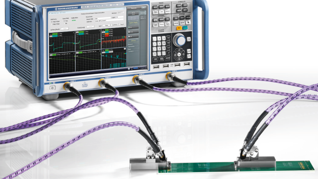
ZNB20 setup to verify the high-speed differential signal lines on a PCB up to 20 GHz
R&S®ZNB20 setup to verify the high-speed differential signal lines on a PCB up to 20 GHz

Your task

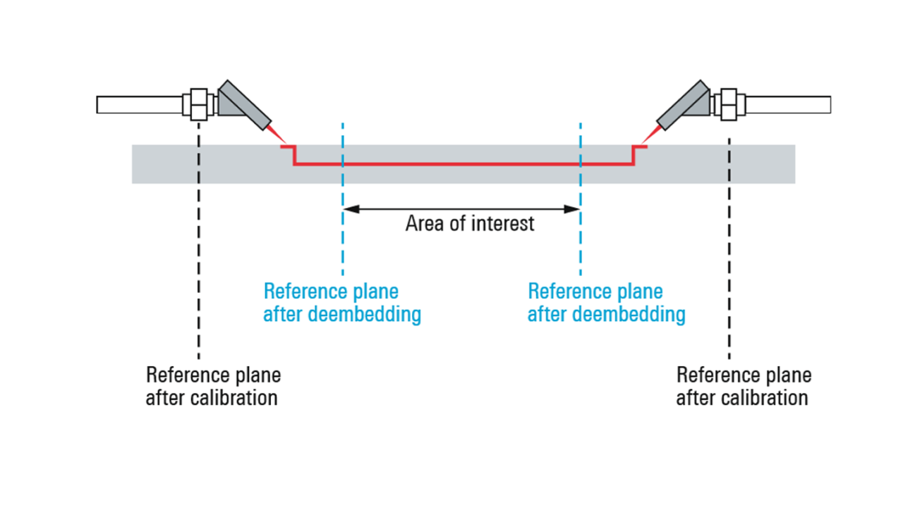
When performing tasks such as verifying digital highspeed signal structures on PCBs, measurements have to be carried out on certain layers without the effects of probes, probe pads, vias, lead-ins and lead-outs. This requires the use of accurate deembedding algorithms to calculate and remove these effects from the measurements, leaving only the result for the area of interest.

Test solution

The setup below shows an example for verifying the highspeed differential signal lines on a PCB up to 20 GHz. The basis of the test setup is the R&S®ZNB20 four-port VNA. Corresponding deembedding tools (e.g. Delta-L, Delta-L+, PacketMicro Smart Fixture Deembedding (SFD) or taiTec In-Situ Deembedding (ISD)) can be run directly on the R&S®ZNB20, eliminating the need for an external PC.

Besides the actual signal trace to be measured, PCB test coupons typically also include a shorter signal trace to facilitate this deembedding. Differential PCB probes (e.g. from PacketMicro) are used to connect the R&S®ZNB20 to these signal traces.

Test setup
Test setup
The steps of the test procedure
Open Lightbox

Process automation

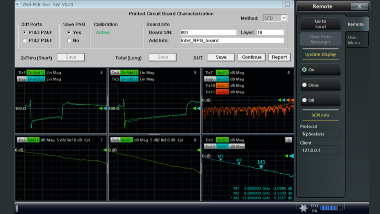
To streamline this procedure and guide the operator through the test steps, the test is typically automated via software. The screenshot on the left shows an example of the three steps of this test procedure:

  • Measurement of a 2×thru (short) structure for deembedding, with results in the left column
  • Measurement of the total (long) structure, with results in the center column
  • Calculation of the area of interest based on the selected deembedding method, with results in the right column

For the 2×thru (short) as well as for the total (long) measurement, the impedance versus time of both probes is displayed above the insertion loss. This makes it easy to quickly identify whether a probe needs to be readjusted.

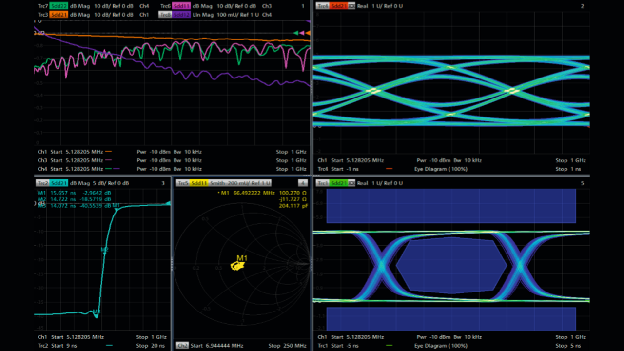
Simultaneous display of eye diagrams and measurements in the frequency and time domain
Open Lightbox

Eye diagram

For further investigations, the R&S®ZNB-K20 option can be used to analyze the eye diagram for the area of interest. This option also allows you to verify the effects of emphasis, noise, jitter and equalization in the eye diagram. It additionally provides a mask test with PASS/FAIL detection and statistic results.

Conclusion

R&S®ZNB offers all the functionality needed to test digital high-speed signal structures on PCBs in one box. Additional deembedding tools can be installed on the instrument to remove the effects of probes, probe pads, vias, lead-ins and lead-outs.

Ordering information
Designation Quantity Type Order No.
Vector network analyzer
Vector network analyzer, 4 ports, 100 kHz to 20 GHz, PC 3.5 connectors 1 R&S®ZNB20 1311.6010.64
Time domain analysis 1 R&S®ZNB-K2 1316.0156.02
Extended time domain analysis 1 R&S®ZNB-K20 1326.8072.02
Calibration unit or calibration kit
Calibration unit, 10 MHz to 24 GHz, 4 ports, 3.5 mm (f) 1 R&S®ZV-Z52 1164.0521.30
Calibration kit, 50 Ω, 0 Hz to 24 GHz, 3.5 mm (m/f) 1 R&S®ZV-Z235 5011.6542.02

Related solutions