Testing insertion loss of PCB signal structures with Delta‑L 4.0
With continuously increasing data rates, signal integrity in high speed digital designs becomes more and more demanding

With continuously increasing data rates, signal integrity in high speed digital designs becomes more and more demanding
PCIe 5.0, for example, provides data rates up to 32 GT/s and defines a maximum insertion loss budget between root complex (RC) and end point (EP). Aside from RC package, EP package, connectors and vias, this is mainly determined by the signal traces on the corresponding PCB layers. Their insertion loss per inch is therefore a key metric and needs to be measured without the effects of any lead-ins and lead-outs, which may include PCB probes and vias. Delta L is an algorithm that provides an easy method of removing those effects and calculating the insertion loss per inch of a PCB trace from measurements of test coupons with different lengths.

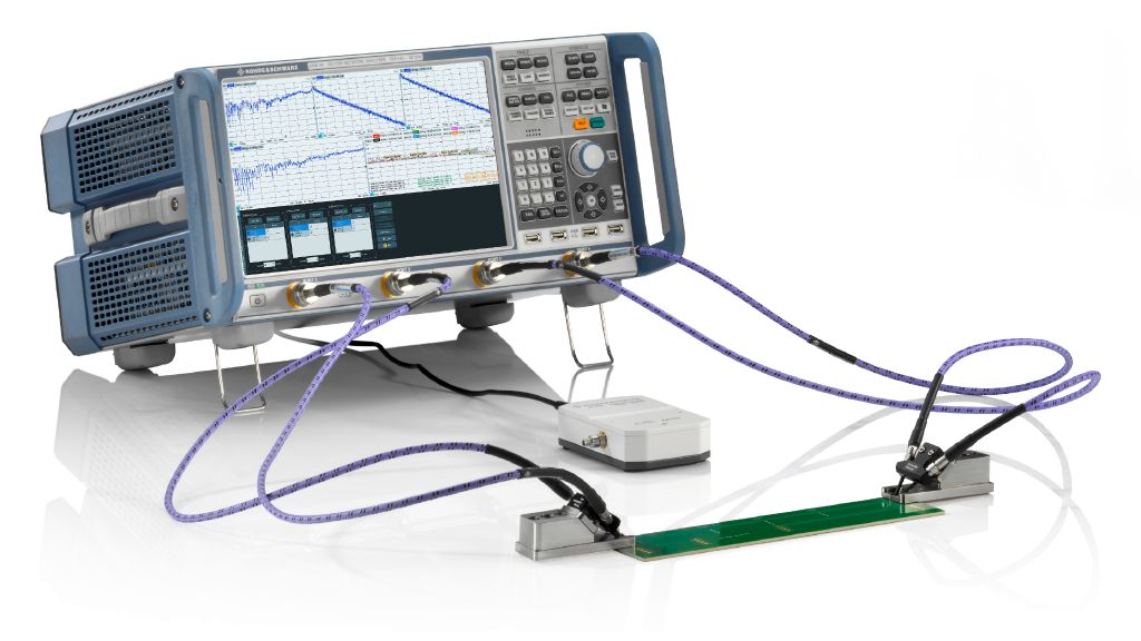
Figure 1: R&S®ZNB40 setup with Delta‑L 4.0 probes
For verifying the insertion loss per inch on a PCB signal trace.
When measuring the insertion loss of a signal trace on a certain PCB layer, the lead-ins and lead-outs including PCB probes and vias produce unwanted contributions to the results and therefore need to be removed from the measurement up to the area of interest. Delta L is an algorithm that has been developed to remove these effects mathematically and calculate the insertion loss per inch of a signal trace on a certain PCB layer, using signal structures of different lengths. The Delta L measurement workflow is fully integrated in the R&S®ZNA, R&S®ZNB, R&S®ZNBT and R&S®ZND vector network analyzers as the R&S®ZNx-K231 option.
A full characterization of a test fixture and the corresponding test fixture deembedding completely shifts the vector network analyzer (VNA) reference plane to a new position next to the device under test (DUT). This method can be used to measure all kinds of DUTs. This is not the case in Delta L, where the algorithm assumes the DUT to be a quasi-ideal transmission line on a certain PCB layer, characterized only by length and loss. The workflow for full test fixture characterization and deembedding is also available in the R&S®ZNA, R&S®ZNB, R&S®ZNBT and R&S®ZND vector network analyzers. Corresponding options are R&S®ZNx-K210 (EZD), R&S®ZNx-K220 (ISD) and R&S®ZNx-K230 (SFD).
In case only the insertion loss per inch on a certain PCB layer is of interest, Delta L provides a straightforward and tailored method to obtain these results by measuring PCB structures with three different methods: 1L, 2L or 3L. These define the number of used test coupons with different trace lengths. Figure 2 shows an example of 2L, using 5 inch and 2 inch test coupons.
Delta L 3.0 defines the probe, probe launch and pitch (1.0 mm) as well as the algorithm to calculate the insertion loss per inch. It works up to PCIe 4.0 and frequencies up to 20 GHz. Delta L 4.0 is a recent extension for PCIe 5.0 and PCIe 6.0, redefining the probe launch and pitch (0.5 mm) as well as extending the algorithm up to 40 GHz. The R&S®ZNx-K231 option includes the new Delta L 4.0 algorithm, which can be used both for Delta L 4.0 and Delta L 3.0 measurements.
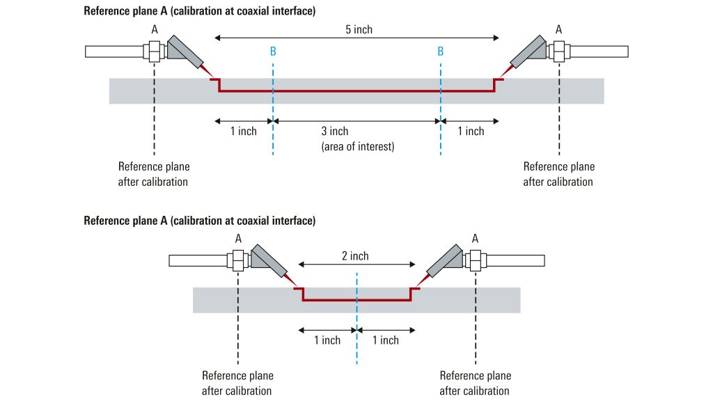
Figure 2: Delta‑L method using test coupons with two different lengths
Shown here: 5 inch and 2 inch test coupons. The insertion loss per inch is determined for the area of interest, here shown as the 3 inch trace segment included in the 5 inch test coupon.

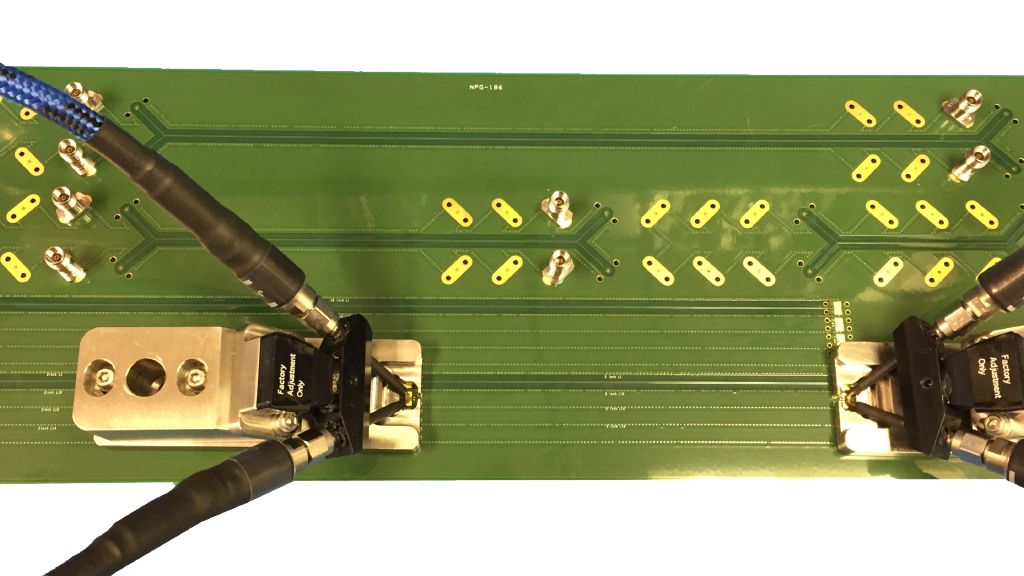
Figure 3: Delta‑L 4.0 probes from PacketMicro
Delta‑L 4.0 probes with guide pins on a test board, including 10", 5" and 2" test coupons on different PCB layers.
The overall setup is shown in Figure 1, a close-up of the used Delta L 4.0 probes and test board is provided in Figure 3, and a further close-up of the probe launch in Figure 4. The VNA is calibrated up to the end of the coaxial cables, e.g. using the automatic calibration unit R&S®ZN-Z54.
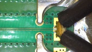

Figure 4: Delta‑L 4.0 probe and test board from PacketMicro
It shows the Delta‑L 4.0 probe launch. Delta‑L 4.0 defines a ground-signal-signal-ground (GSSG) structure with a 0.5 mm pitch, replacing the 1.0 mm pitch of Delta‑L 3.0.
With the R&S®ZNx-K231 option, the Delta L workflow is fully integrated in the R&S®ZNA, R&S®ZNB, R&S®ZNBT and R&S®ZND vector network analyzers. Its implementation supports 1L, 2L and 3L methods, using test coupons with 1, 2 or 3 different lengths. Being integrated inside the instrument, it completely eliminates the need for postprocessing on an external PC.
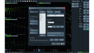
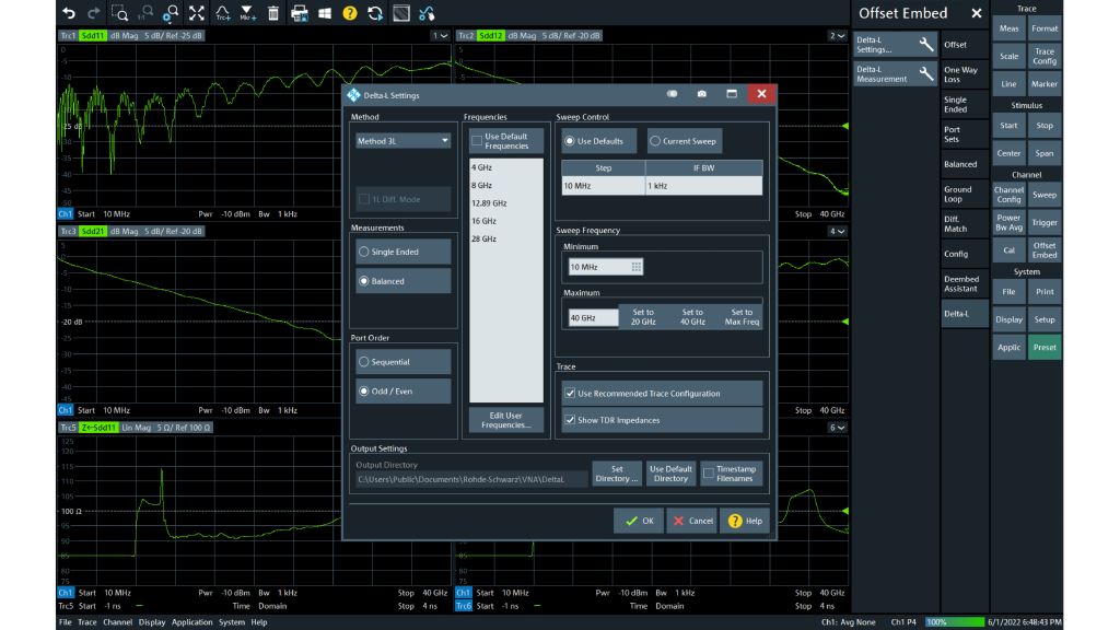
Figure 5: Delta‑L implementation in R&S®ZNx-K231
This implementation supports 1L, 2L and 3L measurement methods.
The dialog shown in Figure 5 and Figure 6 provides access to the Delta L measurement settings, including port configuration of the instrument, selection of the Delta L method and definition of the sweep. Besides the S-parameters, the TDR impedances too can be displayed to verify the proper connection of the Delta L probes and to re-adjust the probes if necessary.
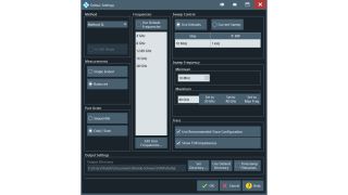
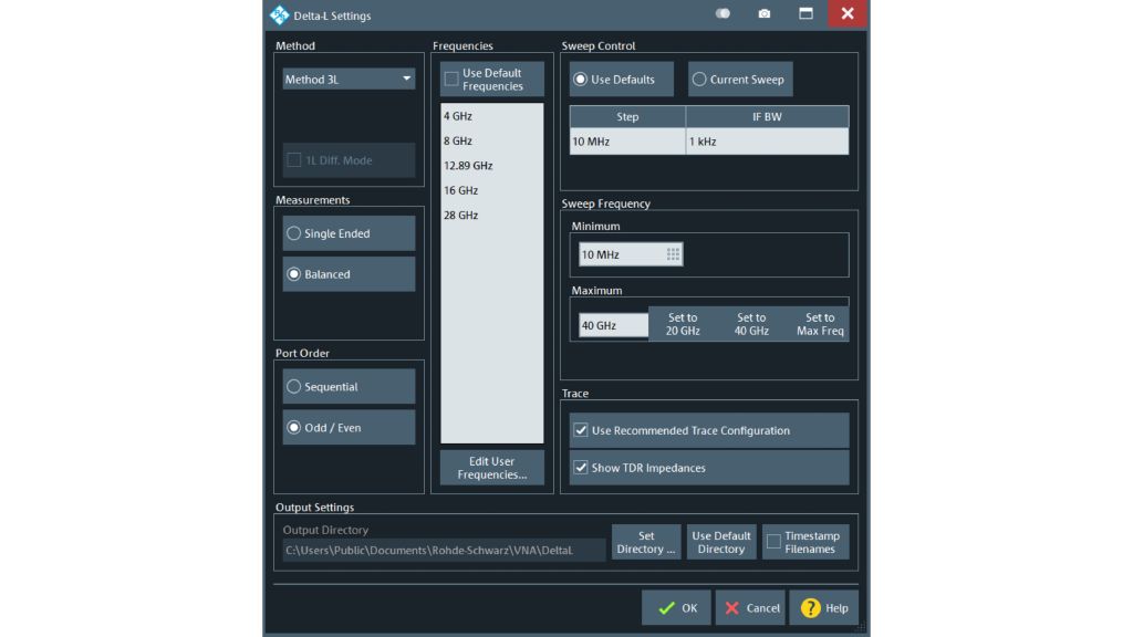
Figure 6: Configuration of Delta‑L settings in R&S®ZNx-K231
Once the user has defined the settings, the Delta L measurement can be started, guiding the user through the different steps of the Delta L workflow. For each coupon length, the user can select a live measurement or load an already existing measurement result saved in Touchstone format.
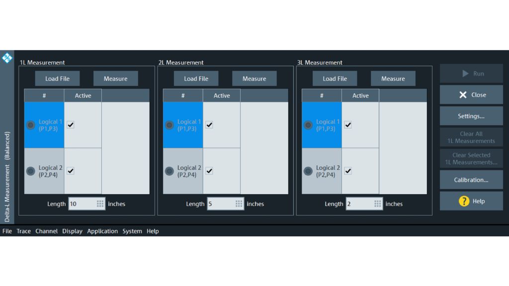
Figure 7: Delta‑L workflow – example for 3L testing
Figure 7 shows an example of the 3L method, where test coupons with 10", 5" and 2" are used. In this case, the Delta L algorithm removes the corresponding lead-ins and lead-outs and provides three results for insertion loss per inch, combining 10" with 5" (area of interest = 5"), 10" with 2" (area of interest = 8") and 5" with 2" (area of interest = 3") as described in Figure 2. The 3L method provides the most information and is typically used in an early phase, e.g. material selection.
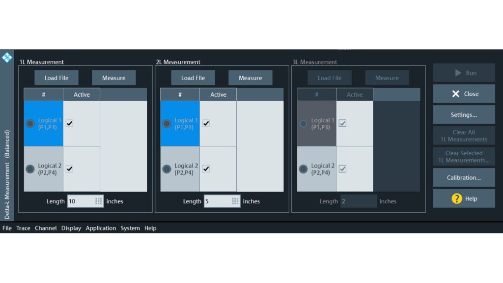
Figure 8: Delta‑L workflow – example for 2L testing
Figure 8 shows an example of a 2L measurement using test coupons with 10" and 5". Here, the Delta L algorithm removes the corresponding lead-ins and lead-outs and provides one result for insertion loss per inch, combining the only available lengths 10" and 5" (area of interest = 5"). The 2L method delivers an accurate insertion-loss-per-inch result in the area of interest and is recommended for board sampling. The 1L method only uses one coupon length and does not remove the lead-ins and lead-outs from the measurement results. It is designed for high-volume manufacturing and provides trends and statistics of the manufacturing process across test coupons on multiple boards.
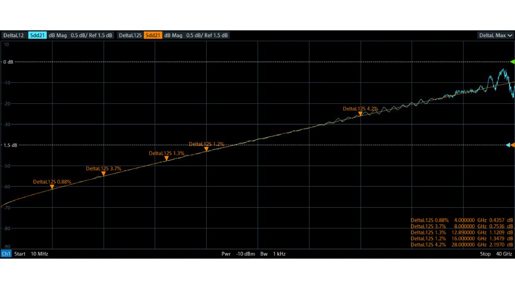
Figure 9: Insertion loss per inch with and without smoothing
As soon as the measurement results of all required test coupons are available, the corresponding Delta L calculation can be started by using the Run button in the Delta L workflow. The results are shown in an additional new diagram. For all the frequencies selected in the Delta L measurement settings, markers are provided showing the numerical values of the insertion loss per inch and the corresponding uncertainty. Figure 9 shows the Delta L results, using the 2L method with a 10" and a 5" test coupon. The orange trace shows the smoothed curve with marker values on the selected frequencies. The blue trace shows the unsmoothed curve for reference and comparison.
The R&S®ZNA, R&S®ZNB, R&S®ZNBT and R&S®ZND vector network analyzers offer all the functionalities needed to perform signal integrity tests on digital high speed signal structures in one box. The R&S®ZNx-K231 option includes the Delta L measurement workflow up to Delta L 4.0 as required for PCIe 5.0 and PCIe 6.0. Delta L 4.0 has been developed for use up to 40 GHz and provides a simple and tailored method to obtain the insertion loss per inch of a trace section on a certain PCB layer.
| Designation | Type | Order No. |
|---|---|---|
| Delta‑L 4.0 PCB characterization, complete 1L, 2L and 3L analysis based on Intel Delta‑L 4.0 methodology | ||
| For R&S®ZNA | R&S®ZNA-K231 | 1339.3922.02 |
| For R&S®ZNB | R&S®ZNB-K231 | 1328.8628.02 |
| For R&S®ZNBT | R&S®ZNBT-K231 | 1328.8663.02 |
| For R&S®ZND | R&S®ZND-K231 | 1328.8705.02 |