When you need an ideal clock source
Today’s digital designs and high-speed data converters require clean clocks with minimal jitter

Today’s digital designs and high-speed data converters require clean clocks with minimal jitter


The R&S®SMA100B provides extremely clean clock signals
Modern digital designs and data converters can only work as well as the clock source allows. To bring out the best performance of a data converter design, an ideal clock source is required to minimize any influence on the signal purity of a digital-to-analog converter (DAC) output or the sampled data of an analog-to-digital (ADC) converter. As clock rates increase, the requirements for signal quality remain or become even more demanding. The bottom line is that you need a flexible clock source that can provide the signals needed for today’s and tomorrow’s designs with minimal jitter and noise as well as best spectral purity.
The R&S®SMA100B produces cleanest signals, which are ideal as a clock source. With an RF output frequency up to 20 GHz, it covers even the latest and next generation DACs and ADCs with steadily increasing clock rates:
❙ Frequency coverage: 8 kHz to 3/6/12.75/20 GHz
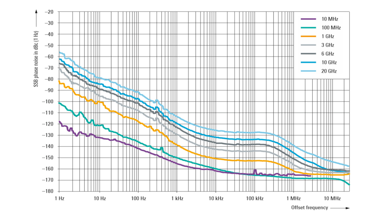
❙ Excellent SSB phase noise: –152 dBc (1 Hz) at 1 GHz, 20 kHz offset
❙ Minimal jitter: 17.5 fs at 1 GHz (1 Hz to 10 MHz bandwidth)
❙ Virtually no wideband noise: –162 dBc at 10 GHz, 30 MHz offset
Lowest wideband noise in particular is of interest for use as a clock source. In applications such as analog-to-digital converter (ADC) testing, the wideband noise of the clock signal can be accumulated multiple times. This causes a degradation of the total signal to noise ratio and therefore needs special attention.
A flexible clock source needs to provide the best RF performance across the entire frequency range since even high-speed devices are characterized and specified at lower frequencies. The R&S®SMA100B uses a direct concept all the way down to 8 kHz, ensuring the best RF performance across the entire range.
In the past, filters were often required in order to suppress harmonics and subharmonics. Such filters can be eliminated thanks to the R&S®SMA100B generator’s built-in harmonic filter and excellent subharmonic suppression:
❙ Harmonics suppression of 70 dB over a wide frequency range
❙ Nonharmonics below –110 dBc at 1 GHz
Sometimes test setups require more cabling than is ideal, resulting in high attenuation. The higher the clock frequencies, the more important this becomes. The R&S®SMA100B offers enough reserves to compensate for losses, making external amplifiers unnecessary:
❙ Up to 38 dBm with the 6 GHz instrument
❙ Up to 32 dBm in the microwave frequency range with the 20 GHz instrument
Thanks to the unique electronic attenuator, the instrument offers high level agility without any wear and tear.


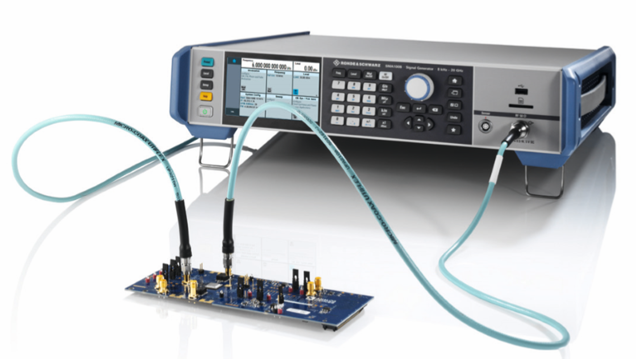
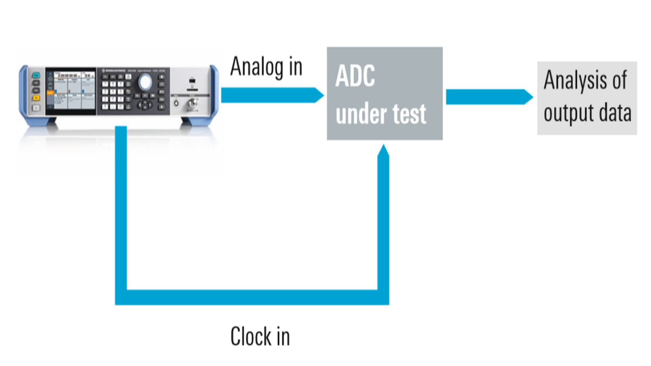
Compact ADC test setup with a single R&S®SMA100B with an integrated second source
A specialty of the R&S®SMA100B is the ability to include an optional second very pure source up to 6 GHz in the same housing (R&S®SMAB-B29 option):
❙ SSB phase noise: –145 dBc (1 Hz) at 1 GHz, 20 kHz offset
❙ Lowest wideband noise: –166 dBc at 1 GHz,10 MHz offset
The frequency and level are completely independent of the RF output. This comes in very handy when testing ADCs since one instrument supplies both the RF input signal and the clock signal. The output can be a standard sine wave or a square wave. To allow direct connection to the DUT, the output supports single and differential format with the ability to add a DC offset. The second source is useful in many ways, because it offers flexible level and frequency at its output.
It is easy to upgrade from your current clock source solution. The R&S®SMA100B supports remote programming emulation of many common platforms of various vendors. With its compact 2 HU form factor, the R&S®SMA100B conveniently fits into any open spot.


Measured SSB phase noise at the RF output of the R&S®SMA100B with R&S®SMAB-B711 option